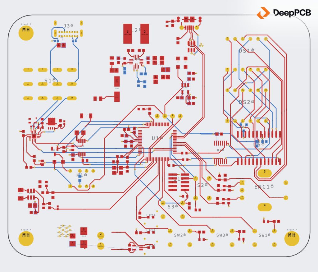

All 342 connections complete in 7 min 44 s. Left to run to 40 min 30 s, it cut the vias from 122 to 94.
Open the routed board in DeepPCB: https://app.deeppcb.ai/shared/bCIeIdKWhNz-CbYFHBXbfAr9ST5cjGde4bfNgI3iD4I

A 4-layer USB-C Power Delivery sink, with a microcontroller, current sensing and a relay-switched load. It has 106 nets and 342 connections. Zach Peterson’s community sent it in for our episode of Altium’s OnTrack podcast, and it’s the board we set up live on air.
The board isn’t ours, so we’re not sharing the design file. The link above opens our routed result.
The result at a glance
Routed in July 2026 by our engineer, before the recording, on the board as submitted apart from the changes listed below. On air we set it up again from the start.
| Result | |
|---|---|
| Connections complete | 342 of 342 (100%) |
| Already connected at import | 156, through the copper the designer left in place |
| First reached 342 | 7 min 44 s (revision 19) |
| Improved route, after running longer | 40 min 30 s (revision 74) |
| Vias | 94, including the designer’s 17 |
| Total track length | 2,085.45 mm, including the designer’s 100.15 mm |
| Routing the whole board by hand | 32 to 40 hours (4 to 5 working days), our engineer’s estimate |
| Manual engineer cleanup still needed | 8 hours, our engineer’s estimate |
Everything was connected by revision 19. The run kept going, and by revision 74 it had brought 122 vias down to 94 and cut the track from 2,245.54 mm to 2,085.45 mm.
What we changed before the run
- We kept the USB pair, which the designer routed by hand. We deleted the rest of the designer’s tracks and all but 17 of the vias. The copper pours on the outer layers and the planes on the two inner layers stayed in place.
- DeepPCB takes a single preferred width from Altium’s width rule. We lowered it from 0.3 mm to 0.254 mm. The vias stayed as the designer set them, a 0.5 mm pad with a 0.2 mm hole.

What Cooper set up
- Both inner layers, GND and PWR, had planes poured but were typed as signal. Cooper set them to power, so the router treats them as reference planes and keeps signals on the outer layers.
- Cooper also proposed wider classes for the power nets. We gave it the widths we wanted instead: 3V3 at 0.3 mm, VBUS at 0.45 mm and ground at 0.3 mm. It made two classes, put the other two ground nets, GNDc and GND_LOAD, in with 3V3 and GND, and said it had done so. It also asked whether the other VBUS nets should join the VBUS class.

Same board, no setup
We also ran this board without Cooper. It connected everything too, but with both inner layers still typed as signal it ran traces through them, and every net came out at the same width.

What we didn’t do
- We didn’t route the USB pair. We kept the designer’s.
- Eight power nets Cooper had proposed widening stayed at the default width: 5V, USB_B_5V, PD_5V, PD_LOAD, VBUS_LOAD, VBUSc, VBUScs and AVDD. We didn’t take that up on this run.
- On import, DeepPCB set aside one clearance rule and the object-type clearances in four others, because it doesn’t read how they’re scoped yet. The net-class clearance, 0.15 mm, applies instead. It also approximated the board’s arcs and left out two pads whose shape it can’t import.
- During the run the router skipped the board’s decoupling-capacitor rules, reporting that their nets could not be routed.
- It isn’t a finished board. Our engineer estimates 8 hours of manual cleanup to finish it. The estimate for routing it by hand covers the whole board, including the parts the designer had already done.
See it on air
We set this board up again, live, in our episode of Altium’s OnTrack with Zach Peterson, from 25:28.
Watch: https://www.youtube.com/watch?v=apvE_ElRhiA&t=1528s
Listen: https://podcast.altium.com/e/ai-pcb-routing-without-the-epic-fails-inside-deeppcb/
More on the episode: https://deeppcb.ai/natural-language-pcb-routing/