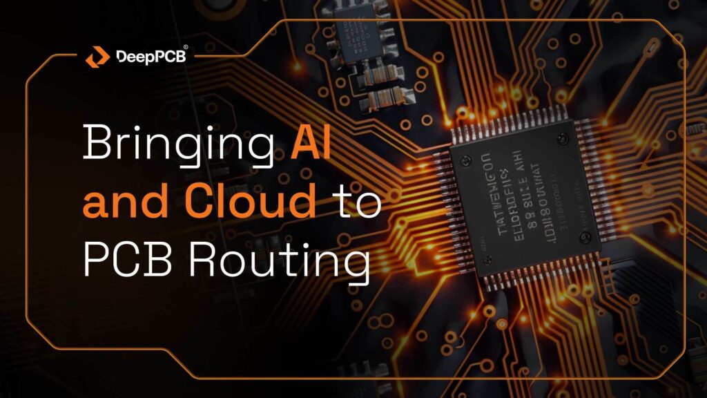
Bringing AI and Cloud to PCB Routing
Revolutionizing PCB Design with AI
From smartphones to life-saving medical devices, most electronic products rely on a hidden gem: the printed circuit board (PCB). These small but mighty boards function as the nervous system in electronic devices, connecting critical components and driving technological innovation.
Given their importance, designing and manufacturing high-quality PCBs quickly and reliably is crucial. This is where artificial intelligence (AI) is revolutionizing a typically slow, manual and highly complex process. InstaDeep, in collaboration with Google Cloud, has developed DeepPCB. This innovative solution empowers designers to achieve unprecedented levels of speed, precision, and efficiency, in crafting these essential components.
For readers unfamiliar with PCB design terminology, we’ve included a glossary at the end of this article.
The Limitations of Traditional PCB Design
For years, PCB designers have grappled with the challenges of manual placement and routing. While traditional autorouters offer some assistance, they fall short, particularly when dealing with advanced features like power planes or differential pairs. It’s akin to a self-driving car that ignores traffic signals—impressive at first glance, but ultimately impractical. Consequently, the sector faces several key challenges:
- Wasted Engineering Time: Highly skilled engineers often find themselves tied up with repetitive tasks, detracting from opportunities for innovation and experimentation.
- Suboptimal Performance: Manual routing frequently struggles to achieve optimal levels of WPP efficiency.
- Manufacturing Challenges: Designs can unintentionally violate manufacturing constraints, leading to compliance issues and production delays.
The global pandemic brought these issues into sharp focus. Supply chain disruptions led to a severe shortage of semiconductor chips, essential components for PCBs. This scarcity caused delays across various industries, from halting automotive production lines to stalling the manufacture of consumer electronics like laptops and washing machines (World Economic Forum) (J.P. Morgan | Official Website).
Beyond highlighting the critical importance of PCBs, this situation emphasized the urgent need for reliable and diversified production methods. DeepPCB was developed in response to this necessity, ensuring fast, efficient, and high-quality PCB design and manufacturing.
Breakthrough in AI-powered placing and routing: PCB designs delivered in a few hours
DeepPCB is a cloud-native, fully automated PCB design platform, built on Google Cloud’s robust infrastructure, that supports designers and businesses in accelerating their PCB product development cycles.
It leverages the power of reinforcement learning, a technique where AI learns – through trial and error – to place and route PCBs faster and more accurately than traditional methods. This means that you can get PCB design solutions in just a few hours instead of the usual days or weeks for complex boards.
This acceleration to the prototyping phase means quicker testing, refinement and getting products to market faster. And for DeepPCB users, the process is straightforward. First, upload your file. Then, you can select the job you need: placement, routing, or both. Finally, download your completed design within the time budget you assigned to the job–typically a few hours.
Accelerating PCB Design Cycles with Tangible Improvements
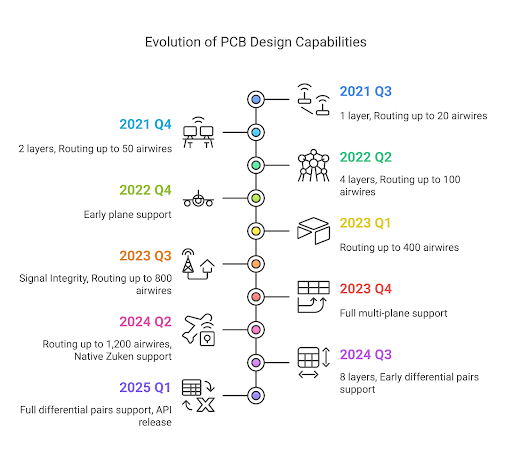
Since its launch, the team has been dedicated to enhancing the platform’s capacity to manage more complex boards, supporting a growing number of airwires and layers. They also actively engage with the PCB design community, continuously learning and adding new features to refine the design process. DeepPCB now handles critical aspects like Design Rule Checking (DRC), net clearance matrices, differential pairs, and power plane area maximization.
Continuous improvement for industrial optimisation
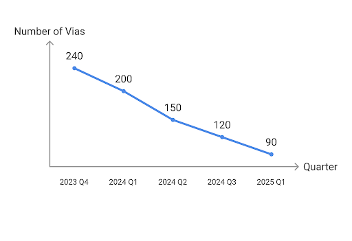
One key PCB that the team uses for benchmarking the increasing power of the platform is a board with 444 airwires divided up into 157 nets, over two layers. This board is representative of typical designs, with some complexity embedded in the connections.
A year ago, DeepPCB successfully routed this board and has since continually refined its solutions, significantly reducing the number of vias—small holes in the PCB that allow connections between its different layers. While necessary, vias can introduce electrical noise and increase manufacturing complexity and cost. Over the past year, the platform has achieved a remarkable reduction of over 50% in via count, leading to a more efficient and cost-effective design.
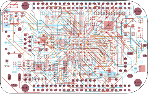
Building on this success, the DeepPCB team is now tackling an even more complex challenge: the BeagleBone Black board. With its 6 layers, 1,223 airwires, and 310 nets, this board is pushing the AI tool to new heights.
A scalable platform with Google Cloud
DeepPCB’s success is underpinned by the robust and scalable infrastructure provided by the Google Cloud Platform. Using InstaDeep’s AIchor platform with Google Kubernetes Engine (GKE) clusters, reinforcement learning workloads are efficiently distributed using Ray, an open-source framework for distributed computing. The integration of KubeRay’s RayJob and RayCluster simplifies this process, allowing KubeRay to automatically spawn the necessary Kubernetes pods (Ray nodes) and seamlessly connect them to the Ray head node. This streamlined setup accelerates the deployment of distributed training jobs, enhancing the ability to deliver rapid results to users.
Combining KubeRay with GKE’s node autoprovisioner on AIchor significantly expedites experiment benchmarking processes. This configuration enables effortless comparison of performance across different machine families and scales. While Kubernetes node autoprovisioners are available on other cloud platforms as well, GKE’s implementation works in tandem with KubeRay to request nodes based on the specified machine family. It intelligently selects the optimal machine size that aligns with the compute resource requirements of each job. This dynamic scaling ensures efficient resource utilization, reducing overhead and improving cost-effectiveness.
Combining GCP’s GKE with AIchor allows for experimentation with various hardware configurations and CPU scales in a controlled environment. This flexibility is instrumental in measuring cost-performance trade-offs, optimizing production processes to deliver the best value to customers. By fine-tuning the infrastructure, DeepPCB reinforces its commitment to lowering the financial barriers to entry for PCB routing and placement design. This strategic use of Google Cloud’s capabilities not only enhances service efficiency but also contributes to making advanced PCB design accessible to a broader audience.
Independent benchmarks show that Google Cloud delivers significant efficiency gains, which translates into real-world benefits for product users. For instance, the new Z3 instances demonstrate a 24% increase in throughput for mixed workloads compared to the previous N2 generation, providing substantial improvements in compute speeds and performance. Additionally, Google’s Cloud TPU v4 outperforms its predecessor by 2.1x on a per-chip basis, achieving better performance and energy efficiency. These enhancements not only result in faster processing times but also lead to cost savings, making Google Cloud an excellent choice for compute-intensive tasks.
DeepPCB – Free to Try and Available to All
One of DeepPCB’s key goals is to make efficient routes to market accessible and affordable for smaller organizations, startups, and less wealthy communities. The platform’s intuitive interface makes it easy for designers of all experience levels to harness the power of AI.
With a free trial available and a flexible pricing structure, you only pay for what you need and use. This approach means that progress is accessible without a hefty price tag. Because the more minds that can create without compromise, the more can be achieved.
For those interested in the way DeepPCB’s AI finds solutions and refines them, intermediate versions of the routings are available for visualization and download.

DeepPCB also Integrates with your Tool
If you’re designing boards on your own software, the team is happy to help you access DeepPCB via API call–letting you query the AI PCB designer in the way you see fit, directly from your tool.
The Future of DeepPCB: Developing a Tool Fit for Purpose
InstaDeep continuously improves DeepPCB, inviting user feedback to ensure optimal usability. InstaDeep’s expertise in AI innovation for Industrial Optimization, including their collaboration with Deutsche Bahn on railway operations, ensures that even greater things are coming for DeepPCB.
>> Try DeepPCB and bring your designs to life faster and more efficiently at DeepPCB.ai. Stay connected with us on LinkedIn and X for the latest updates, and meet the brilliant minds behind DeepPCB at Hardware Pioneers Max on April 23rd and 24th in London, UK, and at PCBEast in Boxborough, MA, USA, on April 30th!
Glossary of Terms
- Routing: Connecting components on a PCB with traces.
- Airwire: A connection that needs to be made between two points on a PCB.
- Via: A small hole in a PCB for electrical connections between different layers.
- Differential Pair: Conductors carrying equal and opposite signals to reduce noise and improve signal integrity.
- Plane: A large copper area on a PCB for ground or power connections.
- DRC-Clean: A design that complies with all specified design rules.
- Autorouter: A tool for automatically routing electrical connections on a PCB.
- Placement: Arranging components on a PCB.
